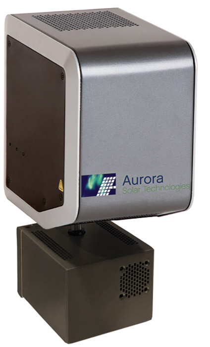
Aurora DM-110s
Inline Non-Contact Emitter Sheet Resistance Measurement
The DM-110s accurately and reliably measures emitter sheet resistance inline at full production speeds. The sensor uses safe reflected infrared light to produce high-resolution characterization of emitter sheet resistance on crystalline silicon wafers.
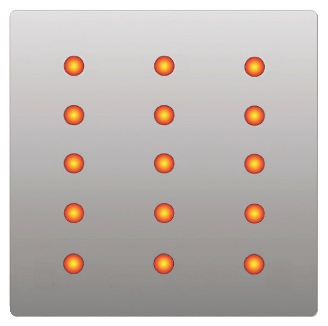
Representative Measurement Pattern
The DM-110s measures the emitter sheet resistance within crystalline silicon photovoltaic (PV) wafers. This innovative product is the industry’s most accurate and reliable measurement tool that characterizes diffusion and annealing process results. The DM-110s measures sheet resistance at a series of discrete points on each wafer, as presented by an automated wafer handling system. Its patented technology provides accurate real-time measurements for process control and optimization.
The system can connect to the Aurora’s VisualizeTM quality control system for integration of measurements with process tools to provide real-time 3D visualization of intra-furnace dynamics, both spatially and by time. This enables optimization of diffusion and annealing processes.
The DM-110s, along with Aurora’s VisualizeTM and ADMTM Control products is designed to enable best practices in sheet resistance quality and process control, supported by Aurora’s industry leading expertise in PV cell fabrication process control.
Features
- Non-contacting continuous emitter sheet resistance
- Designed for sample-based wafer measurement
- Rock-solid long-term measurement stability
- Highly accurate and repeatable
- Compact and easily installed
Benefints
- Allows true characterization of both short – and long-term furnace behaviour
- Eliminates operator error and inconsistencies in offline measurement
- Minimizes wafer damage caused by handling and four-point probe contact measurement
- Reduces labor costs associated with offline sampling and SPC charting
- Rapid payback
- Simplify production quality and process control operations