Products
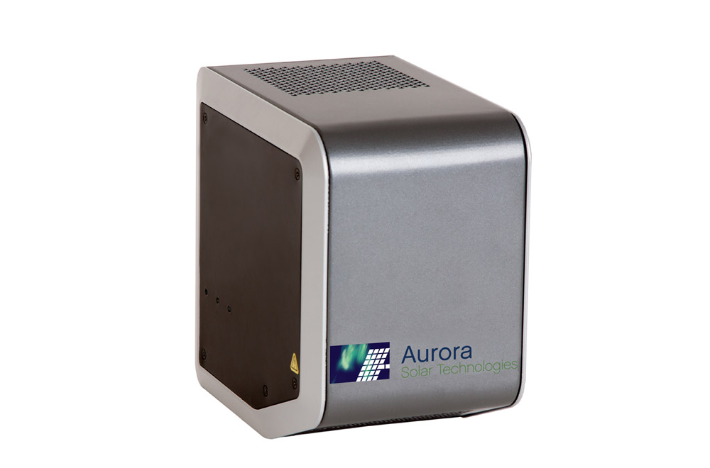
DM™ and TCM™ Instruments
Non-contact measurement of key wafer properties accurately and reliably at full production speeds
The DM sensors use safe infrared light to measure key properties of crystalline silicon photovoltaic (PV) wafers. These innovative products are the industry’s most accurate and reliable measurement tools for characterizing PERC and other high-efficiency cell production processes.
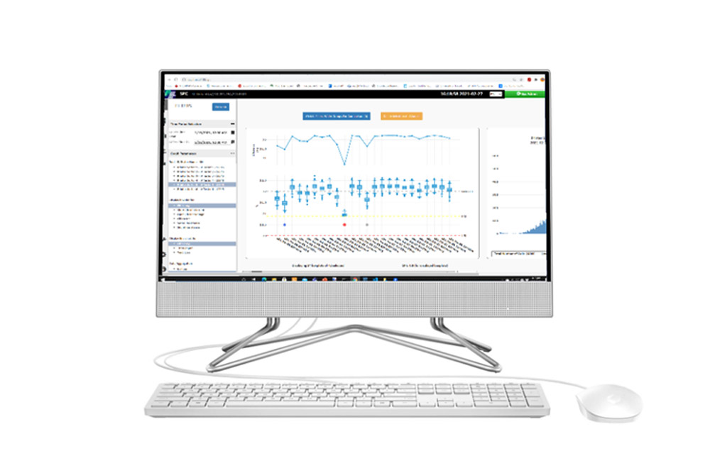
Insight™
Simplify experimentation, maximize yield and increase average cell performance in high-volume cell manufacturing lines
Designed for use in PERC and other high-efficiency cell production lines ,Insight directly addresses the growing challenges facing cell manufacturers in characterizing and controlling production variation. These variations cause yield limitations and profit loss, and can introduce excess warranty liabilities, due to poor electrical performance and other variances in finished cells.
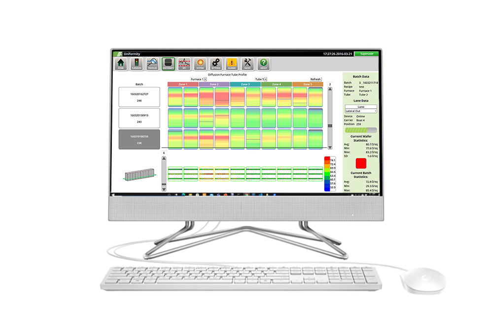
Visualize™
Real-time visualization of critical cell fabrication processes
Visualize enables the optimization and control of critical processes by providing operators and process engineers with real-time 3D visualization of intra-furnace dynamics, both spatially and by batch. By combining DM measurement data with wafer tracking information, Visualize can provide comprehensive historical trending and analysis of key process output parameters along with statistical process analysis.
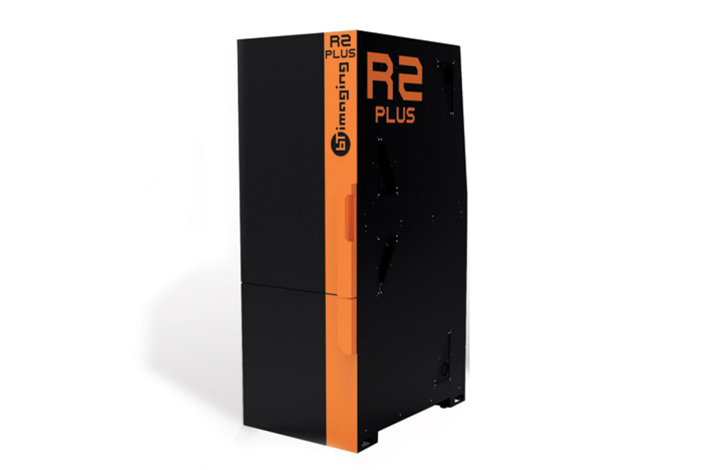
BT Imaging
BT Imaging offers offline and inline photoluminescence inspection equipment for PV materials including silicon, perovskite and thin film materials for use at different processing stages from ingots, as-cut wafers and cells, to solar modules. BT Imaging products are owned and actively used by the world’s top-tier manufacturers and research institutes for research purposes, test and classification, quality control, process improvement and the tuning of production lines.