Aurora TCM-320i/TCM-321i
Inline Non-Contact Bi-facial Transparent Conductive Oxide Measurement
The TCM-320i/TCM-321i system accurately and reliably performs simultaneous measurement of front and rear transparent conductive oxide (TCO) layers on silicon substrates. This unique system operates inline at full production speeds. The sensor uses safe infrared light to produce high-resolution characterization of TCO sheet resistance and thickness from edge-to-edge on a wafer.
DM-321 Measurement Pattern
Description
The DM-321 system measures the front and rear TCO sheet resistances and thicknesses on silicon photovoltaic (PV) wafers. This innovative product provides the industry’s only means to measure these properties in heterojunction technology (HJT) cell production lines. Both sheet resistance and thickness are measured at a series of discrete points along the centerline of each wafer. The DM-321’s patented technology provides accurate real-time measurements for process control and optimization.
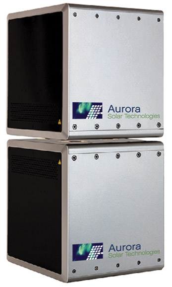
The system consists of a specialized pair of DM-300 series measurement heads, designed as a unit to fit above and below a wafer conveyor, and measures 100 percent of wafers at full production line speeds. The system can connect to Aurora’s Visualize™ quality control system for integration of measurements with process tools to provide real-time 3D visualization of intra-tool dynamics, both spatially and by batch. This enables optimization of PVD or RPD processes.
Features
- Non-contacting continuous TCO sheet resistance and thickness measurement
- Both front and rear layers measured simultaneously
- Designed for 100% wafer measurement up to 5000 wafers/hour
- Rock-solid long term measurement stability
- Encoder controlled measurement triggering
- Highly accurate and repeatable
- Compact and easily installed
Benefits
- Allows true characterization of both short and long term furnace behavior
- Eliminates operator error and inconsistencies in offline measurement
- Minimizes wafer damage caused by handling and four-point probe contact measurement
- Reduces labor costs associated with offline sampling and SPC charting
- Rapid payback
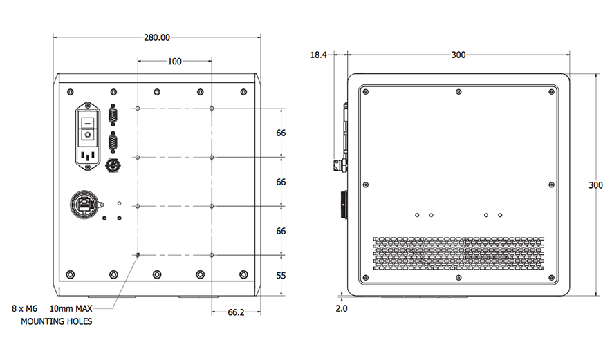
Specifications